


53
CHAPTER 3 SPECIFICATIONS
3
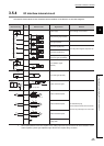
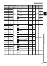
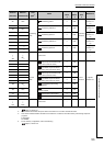
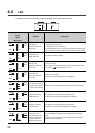
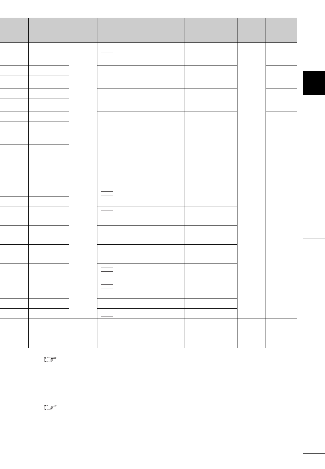
3.7 List of Buffer Memory Addresses
*1 For types of data, refer to the following.
Page 73, Section 5.1
*2 Default values are set after the power was turned off and on or the CPU module was reset.
*3 This column indicates whether the data can be read from or written to the buffer memory area through sequence
programs.
R: Readable
W: Writable
*4 For the memory configuration, refer to the following.
Page 47, Section 3.6
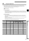
301
12D
H
Positioning
data
Positioning pattern
0R/W
Positioning
data area
Page 82,
Section 5.4
(1)
302
12E
H
Positioning address P1
0R/W
Page 83,
Section 5.4
(2)
303
12F
H
304
130
H
Positioning speed V1
0R/W
Page 84,
Section 5.4
(3)
305
131
H
306
132
H
Positioning address P2
0R/W
Page 84,
Section 5.4
(4)
307
133
H
308
134
H
Positioning speed V2
0R/W
Page 84,
Section 5.4
(5)
309
135
H
310
136
H
System area
•••
•••
399
18F
H
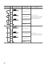
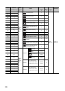
400
190
H
Control
data
Alert output accumulated pulse
setting value (maximum value)
0R/W
Control
data area
Page 89,
Section 5.6
401
191
H
402
192
H
Immediate stop accumulated
pulse setting value (maximum value)
0R/W
403
193
H
404
194
H
Alert output accumulated pulse
setting value (minimum value)
0R/W
405
195
H
406
196
H
Immediate stop accumulated
pulse setting value (minimum value)
0R/W
407
197
H
408
198
H
Accumulated pulse setting
value selection
0R/W
409
199
H
Accumulated pulse error
detection request
0R/W
410
19A
H Measurement start request
0R/W
411
19B
H Reference value write request
0R/W
412
19C
H
System area
•••
•••
1001
3E9
H
Address
(decimal)
Address
(hexadecimal)
Data
type
*1
Name
Default
value
*2
Read/
Write
*3
Memory
area
*4
Reference
Da.1
Da.2
Da.3
Da.4
Da.5
Cd.13
Cd.14
Cd.15
Cd.16
Cd.17
Cd.18
Cd.19
Cd.20